
![]()

🔊 The Complete PCBA Processing Guide: From SMT to Final Testing
Solder Paste Stenciling (The Foundation)
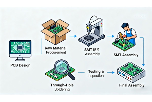
The process begins with applying solder paste to the bare board using a stainless-steel stencil. Accuracy here is vital, as over 60% of PCBA defects originate from poor solder paste deposition. The paste must be perfectly aligned with the pads defined in your PCB design principles.
High-Speed Pick and Place (SMT)
Automated SMT machines pick SMD electronic components and place them onto the solder paste with micron-level precision. This stage is where high-density designs, such as HDI PCBs, achieve their compact form factor.
Reflow Soldering & Thermal Profiling
The board passes through a multi-zone reflow oven where the paste melts to form permanent electrical and mechanical joints. At Topfast, we customize the thermal profile based on the PCB stack-up design to prevent component overheating or “tombstoning.”
Inspection & Quality Control (AOI & X-Ray)
To ensure zero-defect manufacturing, every board undergoes:
- AOI (Automated Optical Inspection): Scans for missing components, polarity issues, or solder bridges.
- X-Ray Inspection: Essential for BGAs and QFNs where solder joints are hidden. This is a standard part of our high-end PCB assembly workflow.
Through-Hole Technology (THT) & Manual Assembly
For components requiring high mechanical strength (like connectors or large capacitors), THT is used via wave soldering or manual soldering. If you’re troubleshooting a prototype, you might need to test capacitors individually to verify circuit integrity.
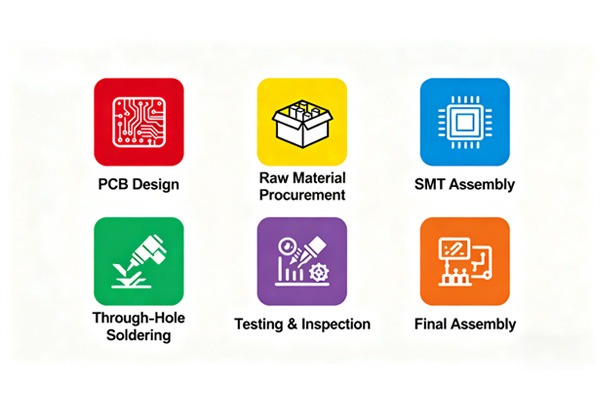
5 Steps to Ensure a Smooth PCBA Processing Flow
- Conduct a Pre-Production DFM Review
Perform a Design for Manufacturing (DFM) check to ensure footprints match your SMD components.
- Optimize the Bill of Materials (BOM)
Verify that all components are available and have the correct manufacturer part numbers to avoid assembly delays.
- Define Solder Paste Requirements
Choose between leaded, lead-free (RoHS), or no-clean solder paste based on the end-use environment of the PCB design.
- Integrate Test Points
Add test points into your layout to facilitate In-Circuit Testing (ICT) and functional verification.
- Final Functional Testing
Once assembly is complete, perform a full functional test to ensure the PCBA meets all electrical specifications before shipping.
Frequently Asked Questions about PCBA Processing
Q: What is the main difference between PCB and PCBA?
A: A PCB is the bare circuit board without components, while a PCBA is the finished assembly with all components soldered and functional.
Q: How can I reduce the cost of PCBA processing?
A: Standardizing component sizes (e.g., using 0603 instead of 0201) and minimizing unique parts in your BOM can significantly lower PCB assembly costs.
Q: Why is X-ray inspection necessary for modern PCBA?
A: It is the only way to inspect solder joints under BGAs or inside HDI PCBs, ensuring there are no hidden shorts or voids.
Q: Can SMT and THT be used on the same board?
A: Yes, this is called mixed assembly. SMT is typically performed first, followed by THT via wave soldering or manual soldering for through-hole parts.
Q: What are the common causes of PCBA failure?
A: Most failures are caused by poor PCB design optimization, incorrect solder paste volume, or inadequate thermal management during reflow.
分享
QUICK GUIDE
SHIPPING METHOD

LEAVE YOUR MESSAGE