
![]()

|
PCBA Capabilities |
|
|
PCB Size |
Max. 610X1100mm |
|
Material |
CEM-1, CEM-3, FR4, Rogers, Al base, FPC, Ceramic, Rigid-flex PCB |
|
Surface Finish |
HAL Lead-free HASL, Falsh Gold, ENIG (Immersion Gold), OSP(Entek), Immersion Tin, Immersion Silver, Hard Gold, ENEPIG |
|
Layer |
1 - 32L |
|
Thickness |
0.2 -6.0mm |
|
Components |
0201, 01005 |
|
Min. pin Space |
0.3mm |
|
Min. Ball Space |
0.3mm |
|
SMD Type |
BGA, WLCSP, QFN, POP, Connectors, wires, cables |
|
SMD Machine Capability |
20,000,000 points/Day |
|
PCBA Electrical Testing |
AOI(100%), X-ray Inspection, ICT (In-Circuit Test)/ Functional testing |
|
Soldering Type |
Lead free Wave Oven, Lead free Reflow Oven, Hand soldering |
|
Other Process |
Three-proof coating, EMS final assembly with enclosure, IC program, function testing, DFM analyse |
|
PCBA Package |
Static bag, Cotton card slot, Carton board slot, Carton board slot with bubble, Custom plastic plate, Custom logo print carton, etc |
|
PCB Capabilities |
|
|
Min. PCB Dimension |
Min. 5*5*0.3mm |
|
Max. PCB Dimension |
1200*650mm |
|
PCB Material |
CEM-1, CEM-3, FR4, Rogers, Al base, FPC, Ceramic |
|
PCB Surface Finish |
HAL Lead-free HASL, Falsh Gold, ENIG (Immersion Gold), OSP(Entek), Immersion Tin, Immersion Silver, Hard Gold, ENEPIG |
|
Chip & IC size |
Min. 0201(0.5*0.25mm) Max. 55mm |
|
Layer |
1 - 32L |
|
Copper Thickness |
Min. base copper: 1 / 4Oz |
|
Max. base copper: 6Oz |
|
|
Max. Aspect Ratio |
12 : 01mm |
|
Hole Size Tolerance |
±0.075(PTH) ±0.05mm(NPTH) |
|
Min. Hole Size |
0.1mm |
|
Min. BGA Size |
0.2mm |
|
PCB type |
Normal through hole, HDI PCB, High Frequency, Buried and Blind vias PCB |
|
PCB Electrical Testing |
Flying probe testing, E-testing jig, Automotic E-testing line |
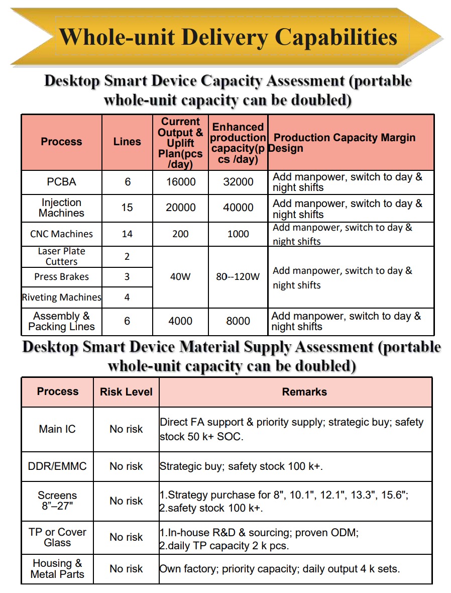
Whole-unit Delivery Capabilities (SKD/CKD is also available)
QUICK GUIDE
SHIPPING METHOD

LEAVE YOUR MESSAGE