
![]()

🔊 The detailed Explanation of PCBA Testing: Production Testing, Functional Testing, Performance Testing
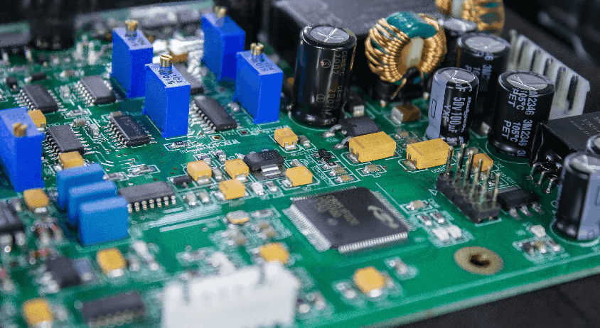
PCBA (Printed Circuit Board Assembly) testing is a critical step in the electronics manufacturing process. Its core objective is to verify the soldering quality, electrical performance, and functional stability of the PCBA, ensuring that the product complies with design specifications and operational requirements.
Products in different application fields (such as consumer electronics, automotive electronics, industrial control equipment, etc.) vary in testing depth and emphasis due to differences in usage scenarios and reliability requirements. However, the core test types are universal. Their specific classifications and details are as follows:
I. Basic Tests in the Production Process (Most Common, Core for Controlling Defects in Production)
-
AOI (Automated Optical Inspection)Purpose: Primarily inspects the appearance integrity and soldering quality of PCBA, serving as the most basic inspection method after SMT (Surface Mount Technology).Key Inspection Items: Missing components, wrong components, reversed components; cold solder joints, solder bridges, component misalignment; abnormal solder joint morphology (e.g., oversized/undersized solder joints, solder spikes, etc.).Features: Fast inspection speed, high efficiency, enabling batch inspection. Usually performed immediately after SMT placement to quickly intercept batch defects visible on the surface, reducing subsequent rework costs.
-
SPI (Solder Paste Inspection)Purpose: Inspects the quality of solder paste printing, a pre-placement inspection to avoid subsequent soldering defects caused by printing issues in advance.Inspection Items: Whether solder paste thickness meets standards; whether solder paste printing position is misaligned; whether solder volume distribution is uniform without missing or excessive printing.Function: Detects printing process issues early, preventing large-scale defects after batch placement and soldering, improving production yield and reducing material waste.
-
X-Ray InspectionPurpose: Inspects solder joint quality on PCBA that is invisible to the naked eye, solving blind spots of conventional optical inspection.Applicable To: Special packaged components such as BGA (Ball Grid Array), QFN (Quad Flat No-leads), CSP (Chip Scale Package), as well as internal solder joint inspection of multi-layer circuit boards.Detectable Defects: Solder voids, pin bridging, cold solder joints (poor connections caused by incomplete melting of solder joints), insufficient solder, and other hidden defects.
II. Electrical Connection Tests (Core for Verifying Circuit Continuity and Component Effectiveness)
-
ICT (In-Circuit Test)Purpose: Inspects the performance of individual electronic components and the integrity of circuit connections on PCBA one by one, locating specific fault points.Key Test Items: Whether parameter values of passive components (resistors, capacitors, inductors, etc.) meet design requirements; polarity and continuity of active components (diodes, transistors, etc.); basic functionality of ICs (Integrated Circuits); presence of open or short circuit faults in the circuit.Advantages and Disadvantages: Advantage – precise fault location, quickly identifying specific defective components or faulty solder joints for easy rework and repair; Disadvantage – requires dedicated test fixtures for specific PCBA models with high upfront investment costs, suitable for high-volume mass-produced products.
-
Flying Probe TestPurpose: Similar in function to ICT, used for inspecting circuit connections and component performance, but without dedicated test fixtures, adapting to small-batch, multi-variety production demands.Features: No dedicated fixtures required, high test flexibility, suitable for PCBA testing in prototype sampling, small-batch production or R&D stages; lower cost than ICT (no fixture investment); however, slower inspection speed, not suitable for efficient testing of high-volume mass-produced products.
III. Functional and System Tests (Core for Verifying Overall Operational Capability of PCBA)
-
FCT (Functional Circuit Test)Purpose: Simulates the actual usage scenario of PCBA to verify whether the entire board operates normally as designed, a critical test step before product delivery.Test Items: Normal power-on startup of PCBA; normal communication functions of various communication interfaces (e.g., UART, I2C, SPI, USB, etc.); normal response of peripherals such as keys, LED indicators, display modules; accurate data acquisition of sensors (e.g., temperature, humidity, pressure sensors); power output meeting design standards.Essence: From the user’s perspective, comprehensively verifies the overall functional integrity and coordination of PCBA, ensuring normal operation after product delivery.
-
Burn-in TestPurpose: Exposes early failure problems of products in advance by operating PCBA for a long time under simulated extreme usage environments, screening out potential defective products and improving long-term reliability.Common Test Conditions: Continuous operation in high-temperature environments; long-term power-on (usually several to dozens of hours); operation under high-load conditions to maximize potential failures.Applicable Scenarios: Products with high reliability requirements, such as industrial control equipment, automotive electronics, power supply products, etc. Burn-in testing reduces the failure rate of products after delivery.
IV. Reliability and Environmental Tests (For High-Requirement Products, Verifying Extreme Environment Adaptability)
-
Environmental TestingMainly simulates the adaptability of PCBA in different usage environments to ensure stable operation in complex environments. Common test items include: high and low temperature cycle test (verifying stability under high and low temperature environments), humidity and heat test (simulating humid and high-temperature environments to prevent component oxidation and short circuits), vibration/shock test (adapting to vibration-prone scenarios such as automotive and industrial applications to prevent solder joint detachment and component damage), salt spray test (for outdoor equipment to prevent PCB corrosion).
-
EMC / EMI TestingPurpose: Verifies the electromagnetic compatibility of PCBA, covering two core dimensions – Electromagnetic Interference (EMI) and Electromagnetic Susceptibility (EMS), ensuring products do not generate excessive electromagnetic interference during operation and can resist external electromagnetic signal interference.Importance: EMC/EMI testing is mandatory for consumer electronics, medical equipment, automotive electronics and other products. Failure to pass the test prohibits product market entry, avoiding interference with other electronic devices or self-failure due to external interference.
V. Software and Program-Related Tests (Easily Overlooked but Critical, Ensuring Program-Hardware Adaptation)
- Programming + Debug Test
Mainly for PCBA requiring firmware burning, ensuring perfect adaptation between programs and hardware. Test items include: firmware burning (writing designed programs into ICs, verifying burning success rate and integrity), Boot test (verifying normal program startup after PCBA power-on without startup failures or freezes), online debugging (troubleshooting faults during program operation to ensure program logic meets design requirements), boundary scan (Boundary Scan / JTAG, detecting IC pins and circuit connections via dedicated interfaces, suitable for debugging high-density packaged components).
VI. Actual Industry Test Flow for Consumer Electronics PCBA (Aligned with Mass Production Practice)
In the mass production of consumer electronics PCBA, the test flow balances efficiency and quality, usually performed in the following sequence to ensure timely interception of defects at each stage. The specific flow is:
SPI (Solder Paste Printing Inspection) → SMT (Surface Mount Technology) → AOI (Appearance and Soldering Inspection) → X-Ray (Hidden Solder Joint Inspection) → ICT/Flying Probe Test (Electrical Connection Inspection; flying probe for small batches, ICT for large batches) → Firmware Burning → FCT (Functional Test) → Burn-in Test → Sampling Inspection (randomly selecting finished products for comprehensive re-inspection to ensure quality consistency of batch products).
Note: The test flow for different product types will be adjusted according to requirements. For example, automotive electronics will add more environmental testing and EMC/EMI testing steps, while industrial control equipment will intensify the rigor of burn-in testing and vibration testing.
分享
QUICK GUIDE
SHIPPING METHOD

LEAVE YOUR MESSAGE